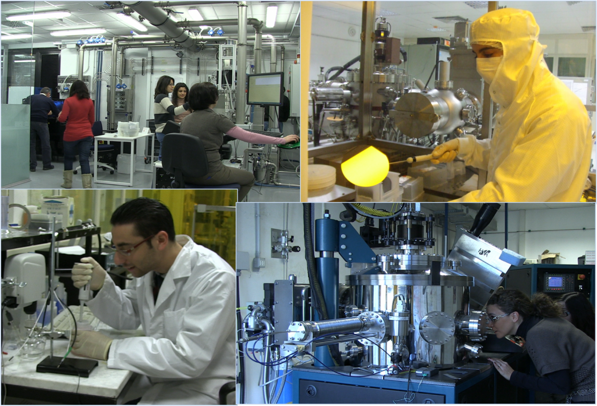
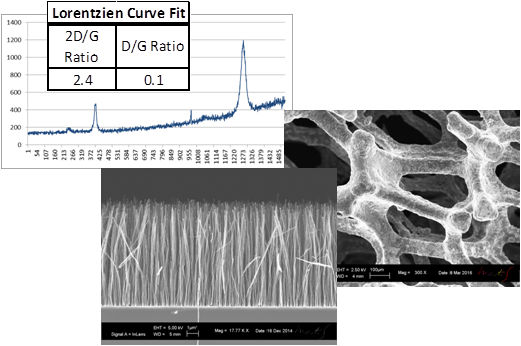
The synthesis of advanced materials is a long standing key activity of the Catania Unit. Several state of the art equipments are installed, as well as many methodologies for the realization of functional advanced materials are developed. All the efforts are devoted to make this Unit an excellence center on these topics, synergistically coordinated with the other Units of IMM. Great interest is pointed towards low dimensional materials (0D, 1D e 2D, 3D) such as metals, oxide and Ge nanoparticles; TiO2, ZnO, CuO, Si, C nanowires, nanotubes and nanorods; graphene and NiO foams. Thin film synthesis is employed for realizing rare earth oxides and silicates, group IV semiconductor QDs in silica, undoped and rare earth doped Si oxycarbide, transparent conductive oxide, calchogenides and functional nanometric oxides. Chemical methods are used for the synthesis of polymeric nanocomposites based on TiO2, ZnO and Graphene. The realization of these materials mainly relies on some leading edge synthesis equipment as reported below.
UHV AJA Confocal RF-Magnetron Sputtering System
- UHV chamber (10-9 mbar)
- Up to 3 targets (4 inches), that can be simultaneously and indipendently used (3 RF and 1 DC power supply)
- Wafers up to 8”, that can be heated up to 800 °C
- 3 gas lines
- equipped with a thickness monitor
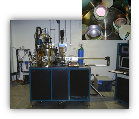
Scope: Deposition of high purity single element or alloys thin films and multilayers with accurate control of stoichiometry and of elemental content (lower than 0.01 at.%). Some examples:
- Rare earth oxides and rare earth silicates (i.e. Y2-xErxSi2O7)
- Undoped and Eu doped SiOC
- GeSbTe and Ge1-x Tex alloys
- Ge and Si1-x Gexthin films and quantum dots
- Ti and TiO2 and Cu2O
- Transparent Conductive Oxide (AZO, ITO, TZO)
Contact: Maria Miritello
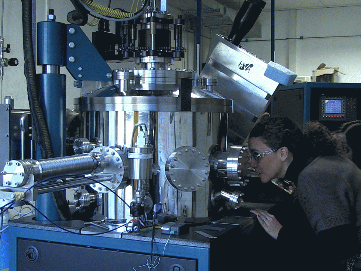
DCA Molecular Beam Epitaxy
- Sample holder up to 1100 °C
- 3 e-gun: Si, Ge, SiC for co-deposition
- 5 effusion cells for doping (B, Er, Sb, Ge, As)
- In situ RHEED analysis
- In situ XPS-UPS-Auger analysis, UV lamp, Flood gun for insulators
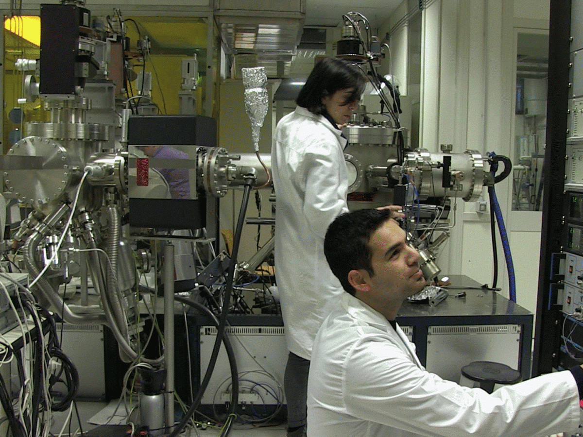
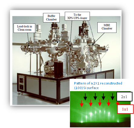
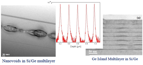
Scope: Synthesis of SiGe quantum wells - Ge quantum dots - Ultrathin doped layers (FWHM 3 nm) - Complex multilayer structures
Contact: Antonio Terrasi
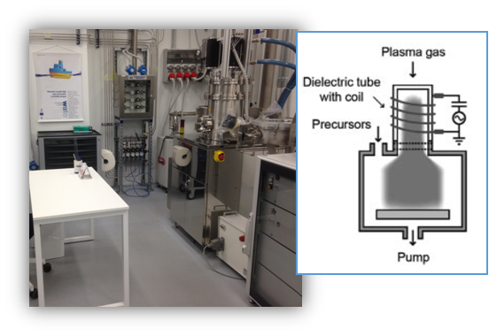
Aixtron-"Black Magic" CVD-PECVD
Thermal and plasma enhanced chemical vapor deposition
- Gas sources: Ar, H2, NH3, CH4, C2H2
- Temperature up to 1000°C
- Ramp up to 300°C/min
- Up to 6’’ wafers
Scope: Synthesis of
- 2D graphene
- 3D graphene based structures
- Carbon nanotubes
Contact: Sabrina Carola Carroccio
Picosun™ R-200 Advanced Atomic layer deposition
- Thermal and plasma (remote) ALD
- Deposition on wafers up to 8” and also on powders
- The sample holder can be heated up to 650 °C.
- The chamber up to 500 °C
- Equipped of quartz balance, RGA, ellipsometer
Scope: TiO2, ZnO , Al2O3 , Ag , Ru , Pt , Pd
Contact: Giuliana Impellizzeri
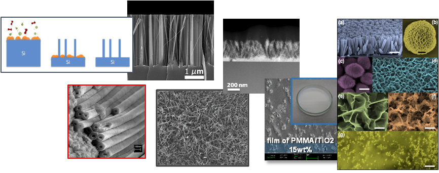
Low cost chemical and physical methodologies
- Synthesis of Si nanowire
- TiO2 nanotubes, nanoplumes and nanowires
- Polymeric nanocomposite
- ZnO nanorods, microflowers, nanoeggs and nanowalls
- NiO nanosheets and nanofoam
- Ge colloids