The workshop is jointly organized by STMicroelectronics and the Institute for Microelectronics and Microsystems of the Italian National Research Council (IMM-CNR). It represents a melting point between the academic and research world and the industrial development in the field of the structural characterization and the microanalysis by electron microscopy (https://www.st.com/content/st_com/en/about/events/events.html/electron-microscopy-workshop.html).
The scope of the event will be focused on new methods applied to semiconductor devices (silicon based, wide band gap, metallic interconnections, nanotechnology, etc) and materials science. It will highlight recent progress in instrumentation, in chemical and structural analysis, in sample preparation by mechanical thinning and by FIB, as well as in situ devices polarization dependent analyses.
The scientific program will be opened by a lectio magistralis delivered by Prof. Giulio Pozzi (Department of Physics and Astronomy, University of Bologna and Ernst Ruska-Centre and Peter Grünberg Institute, Forschungszentrum Jülich) regarding Electron Holography: from the beginning to recent developments. The session will continue with scientific presentations given by researchers coming from STMicroelectronics, IMM-CNR, ENEA, LETI CEA, Cemes CNRS and Companies specialized in electron microscopy.
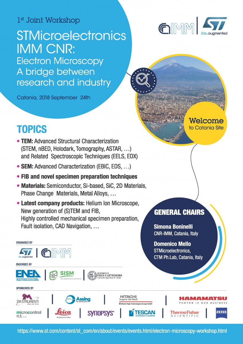
The workshop will present new insights focusing on the following topics:
TEM: Advanced Structural Characterization (STEM, nBED, Holodark, Tomography, ASTAR, …) and related Spectroscopic Techniques (EELS, EDS)
SEM: Advanced Characterization (EBIC, Voltage Contrast, EDS, …)
Novel specimen preparation techniques by FIB
Materials: SiC, Phase Change Materials, Metal Alloys, nanowire, ...
Latest company products: Helium Ion Microscope, New generation of (S)TEM and FIB, Highly controlled mechanical specimen preparation,..